

Mode $19 is "Read DTC Information", so it should return status of every specified DTC. I'm not sure exactly...
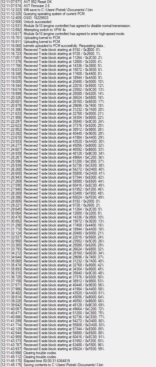
I've made a huge progress last couple of days! E-side SPI comms are finally working and I have working T-side and E-side read software!


Mode $19 is "Read DTC Information", so it should return status of every specified DTC. I'm not sure exactly...
I've made a huge progress last couple of days! E-side SPI comms are finally working and I have working T-side and E-side read software!
First off Congratz dzidaV8. Fantastic that you have the download/upload solved!!
I was asking after Mode 19 because IF it is similar to Mode 18, a whole bunch of memory locations can be identified. There are a number of tables for DTCs that try to classify the use. J2190 calls them up for mode 18 as follows:
bit 7 Warning lamp illuminated for this code
bit 6 Warning lamp pending for this code, not illuminate but malfunction was detected
bit 5 Warning lamp was previously illuminated for this code, malfunction notcurrently detected, code not yet erased
bit 4 Stored trouble code
bit 3 Manufacturer specific status
bit 2 Manufacturer specific status
bit 1 Current code - present at time of request
bit 0 Maturing/intermittent code - insufficient data to consider as a malfunction
If I can say for sure that the status is the same for Mode 18 and 19, the definition of 144 bits become determined. I can't find any definition of Mode $19 and think it may be a GM special/non-standard. I have disassembled and commented the code to the point where this all is taking shape. Just don't know the intent of the code completely.
-Tom
I had a close look at Mode 3C used to read various parameters from the PCM including VIN...
MODE $3C
Mode $3C is loosely defined in SAE J2190. In my PCM (calibration #?16236217?) the request looks as follows:
H0 H1 H2 MODE BLOCK# <CRC>
Header 0: Priority: Any, Three byte consolidated header, IFR not allowd, Physical addressing, Node to Node
Header 1: Target address or destination can be $10 (engine controller) or $FE (all nodes)
Header 2: Source address should be one of the off board tester/diagnostic tool addresses.
For testing I have used $4C $10 $F0 for header values. The Mode I am looking at is $3C.
Supported block numbers are:
$01 through $08, $0A, $0B, $40 through $49, $A0
The data associated with each of the blocks is returned based on a look up table.
TSIDE
Block# Start Data Content
Address Length
$01 $0E24 $06 VIN BLOCK 1
$02 $0E29 $06 VIN BLOCK 2
$03 $0E2F $06 VIN BLOCK 3
$04 $0E04 $04 VIN BLOCK 4
$05 $0E08 $04 VIN BLOCK 5
$06 $0E0C $04 VIN BLOCK 6
$07 $0E10 $04 VIN BLOCK 7
$08 $0E20 $04 VIN BLOCK 8
$0A $2000 $04 Calibration Number (binary)
$0B $0262 $04
$A0 $0E35 $01
ESIDE moved by SPI to Tside RAM
Block# Start Data Content
Address Length
$40 $182A $02
$41 $182C $06
$42 $1832 $06
$43 $1838 $05
$44 $183D $06
$45 $1843 $06
$46 $1849 $05
$47 $184E $06
$48 $1854 $06
$49 $185A $05
One interesting note...
Block $01 is special in that while the LUT calls for 6 bytes of VIN info to be sent there is a special branch for this block only. Block 1 sends the first data as $00 in all cases, followed by the five bytes starting at EEPROM $0E24. It is not clear to me why things were done in this way.
I wonder if a complete map of EEPROM content is available somewhere?
There are 512 bytes of EEPROM in each of the Tside and Eside processors. Has anyone looked into the use of all this?
-Tom
Hi Tom
Did you made any recent progress with the disassmebly?
I have a simple question for your hardware skills.
On eside the main routine that runs the engine is IRQ. Do you know at what rate it runs and what triggers it. Is it some external timer or it is trigger by some opti signal interrupt. It is also intersesting to find the same info for other routines but that one is the most of interest.
Hi Kur4o
I am making progress on the Tside code. I lack knowledge about a number of things
that slows me down, but I am working away at it. I need to find out more about
built in testing. I see references to balance test and others. Work goes on. I
have not posted in a long while and need to get back to that.
I have not yet done a dive into the Eside hardware. I will get back to you in a
couple of weeks with info on what is driving the IRQ pin, and other stuff I
find along the way. Time to clean up my work bench & ...
-Tom
Hi Kur4o,
Had an initial look at your Q... The IRQ is pin 19 on the processor. It tracks to a pull up resistor on the underside and then to the gate array that we have little info on. The gate array house number 16195392 is in a PLCC68 package, IRQ is on
Pin 47.
I will have a better look at this and let you know. I plan to look through the opti connections.
Later I will get round to connecting my opti spark emulator and see the function of the pin on the scope. Probably winter though.
Post a bit more on this soon.
-Tom
Great find.
I suspect it can be driven on a fixed interval rate or some trigger event like opti low pulse signal.
I don`t have enough knowledge on the hardware and processor speed, but how much time it will take for the processor to execute the irq subroutine. I noticed that above 3-4000 rpm some code is omited based on the cyl id. For example each #8 cylinder is fired the ve and spark tables are not refreshed. It is scattered around the code based on different cylinders. It could be the processor is slow enough.
It also doesn`t like jumps out of the routine and turns to crap if a try to add aldl interupts. I guess it is critical time sensitive.
The IRQ seems to be triggered every low resolution opti pulse, I'd have to trace the PCB but my guess is that IRQ pin is driven by TPU chip.Originally Posted by kur4o

In looking at distributor inputs, I am now convinced the Timer Processor Unit (TPU) is involved. That needs to be figured out to have any hope of understanding the heart of the system. The injector timing and spark timing are complex. Also the transmission monitoring is complex. I needed a simple place to start figuring the part out.
In looking through the ESide code, I believe the VATS to be a simple function. From what I see, PCM Connector C1 (RED) pin 25 (BLUE wire) takes a toggle signal from the BCM. The ESide routine that monitors the toggle rate runs at 12.5mS intervals --> 80 times a second. The code tests a register in the TPU against the sample taken in the previous run 12.5mS earlier. In case where there is at least some transitions on the line, it tests the rate. Two thresholds for rate are set in the calibration:
-CALIBRATION: $05B0 1456
-CALIBRATION: $04A8 1192
These may be specific to year/make/model, the above is what I have. All this suggests the nominal frequency sent by the BCM is 50HZ with the right key resistor in place.
The result of all this is a couple of flags are set when the right frequency is sensed.
One is used on the ESide to handle things like dtcs: -DTC P1626: PASS KEY FUEL ENABLE CIRCUIT CLEAR FLAG
and cut off of fuel pump / injectors.
The other is sent to TSide through the SPI byte 3, bit2.
SPI ESide E_Xfr T_Xfr TSide
BYTE03 $005E $0098 $02F3 $00AE
BIT 0 DTC P0200: INJECTOR CIRCUIT CLEAR FLAG
BIT 1 DTC P0200: INJECTOR CIRCUIT SET FLAG
BIT 2 VATS FUEL ENABLE FLAG
BIT 3 DTC P1222: INJECTOR CONTROL CIRCUIT INTERMITTENT CLEAR FLAG
BIT 4 DTC P1222: INJECTOR CONTROL CIRCUIT INTERMITTENT SET FLAG
BIT 5
BIT 6
BIT 7 ESIDE MIL REQUEST FLAG
A Mode $23 command can be sent to read the VATS status. There are probably a bunch of other ways to do this, I only needed 1 to prove things out.
Using an ELM327 for access I sent "23 00 00 AE 01". This is with the header pre-set to "4C 10 F0"
The ECM responds with header: 4C F0 10 message:63 00 AE 04 00 00 00 crc: F8
The way I believe this part of the TCU works is:
CPU runs an oscillator at 12.5829mhz. The E clock is a divide by four 3.145725mhz. This is divided in the TPU by 48 resulting in a sample clock at 65,536hz. A nominal 50hz input will result in a count of 1310 or so. If I am correct in my assumptions, the threshold 1192 would give a top acceptable frequency of just under 55hz. Similarly, the threshold 1456 would give a bottom acceptable frequency of just over 45hz.
The tpu it's self operates similar to the 'hc11 input capture timers. One edge (perhaps the rising edge say) latches the count. The software subtracts the previous value and tests against the threshold.
=======================
Some questions for you all...
- Are all the functions of the TPU documented somewhere? If I knew all the things it does it would be a good help
- Are the connections to the TPU documented somewhere? Looking at the connected pins would help with the first Q
Speculation
- I think the 8bit read followed by a 16 bit read solved a problem of synchronizing between high and low bytes. The first read 8bit latches the value. The second read results in reading high first then low, like a normal 16 operation in an hc11. I expect address 0 is not even connected to the part. I plan to test for this.
=======================
VATS code segment
\Code:VATS code segment 4B6C B6 14 6A LDAA $146A ; READ TPU REGISTER 4B6F FC 14 6A LDD $146A ; 4B72 0E CLI ; ENABLE INTERRUPTS 4B73 37 PSHB ; STACK TRANSITION COUNT LS 4B74 36 PSHA ; STACK TRANSITION COUNT MS 4B75 B3 02 24 SUBD $0224 ; SUBTRACT PREVIOUS COUNT FROM CURRENT 4B78 38 PULX ; TRANSITIONS SINCE LAST TEST 4B79 27 15 BEQ $4B90 ; NO TRANSITIONS 4B7B FF 02 24 STX $0224 ; UPDATE PREVIOUS TRANSITION COUNT 4B7E 1A B3 20 23 CPD $2023 ; CALIBRATION: $05B0 1456 45HZ 4B82 22 0C BHI $4B90 ; 4B84 1A B3 20 25 CPD $2025 ; CALIBRATION: $04A8 1192 55HZ 4B88 25 06 BCS $4B90 ; 4B8A 14 01 80 BSET @$01,$80 ; VATS ENABLE FUEL FLAG 4B8D 14 5E 04 BSET @$5E,$04 ; SPI VATS ENABLE FUEL FLAG
I continue to look at the "TPU" as it appears to be where most if not all of the time sensitive engine controls take place. I began by looking at it's initialization. The manner that it is initialized is the same in code for 1994 through 1997.
I believe the "TPU" is described in a Delco patent. Delco describes the part as a microprogrammed timer processor but throughout the text refer to it as TIO. You can view the patent at: https://www.lens.org/lens/patent/089-678-009-223-680 for confirmation the Patent Numbers: 5,115,513 and/or 5,117,387. They both look to me as the same idea...
The reason I believe this describes the part used in LT1 based vehicles is the description given in "PREFERRED EMBODIMENT" and "Architectural Overview" sections. The following is what I believe and will now seek to confirm. The following details suggest to me that the patent documents the 16195392 / TIO part.
- The size of the microcode store is the same between the patent and the TIO part. The given size is 256 words of 64 bits. The patent states: The microcode store is preferably in the form of a ROM although RAM or other memory technology can be used instead. The TIO uses RAM and configures it with the following sequence:
The microcode is loaded sequentially through four registers at $16E0, $16E2, $16E4, $16E6. Once four words are written, the destination microcode address is written to $1400. This initiates loading of the microcode word into RAM. The above loops through the 256 sixty-four bit words to complete loading the microcode.
The size of both the TIO shared RAM blocks exactly matches the patent. In the patent the combination of both blocks is referred to as "Parameter RAM" comprised of "Temporary RAM" and "Shared RAM". Patent sizes the shared RAM at 128 words by 16 bits and the temporary RAM at 64 words by 16 bits.
The code in the LT1 computers clears both shared and temporary RAM, the sizes match the patent exactly.
In reviewing the code, the patent, the application and what I know of the system, I come to the conclusion that the TIO is described by this patent.
I am most interested to hear if others agree or disagree and if anyone has found a match between the list of fields and the microcode loaded in the software. Here is the list of fields given in the patent:
P2A (9) Parameter to A bus
T2B (7) Temporary to B bus
SUB (1) Subtract/Add
SHC (2) Shift control
PWR (9) Parameter Write address
PWU (1) Write Unconditional
EXC (4) Execute (Branch) Condition
PNS (6) Pin/Flag Select
PAC (2) Pin Action Control
ENA/DIS (2) Enable/Disable
PRB (1) Present/Requested bit
REQ (6) Requested Address and/or Request Flag
DEC/END (2) Decrement/END Register
NAP (8) Next Address Pointer
NIP (4) Next Index Pointer
I am not sure which fields are assigned to which bits. I am trying to analyze that now.
Also there is the question of how the sequence of bytes the software loads are formed into words. Here is what I think:
Stated in the patent & makes sense from a 68HC11 point of view:
Byte0 Byte1:Byte0
Byte1
Byte2 Byte3:Byte 2
Byte3
Byte4 Byte5:Byte4
Byte5
Byte6 Byte7:Byte6
Byte7
This could result in the microcode loading into a 64bit word as:
Alternative 1 Byte7:Byte6:Byte5:Byte4:Byte3:Byte2:Byte1:Byte0
Should the design be consistant with writing high order first:
Alternative 2 Byte1:Byte0:Byte3:Byte2:Byte5:Byte4:Byte7:Byte6
Consider that the word high order first statement in the patent
doesn't apply to microcode loading:
Alternative 3 Byte0:Byte1:Byte2:Byte3:Byte4:Byte5:Byte6:Byte7
I have written a number of C classes to help with the analysis but as yet I can't determine the placement of fields within the microcode or the order that the byte sequence is loaded into the 64bit word. I will keep plugging away at this.
-Tom
 Posting Permissions


 Reply With Quote
Bookmarks